CIQTEK Debuts Self-Developed 200 kV TEM, Launches Five New EM Products
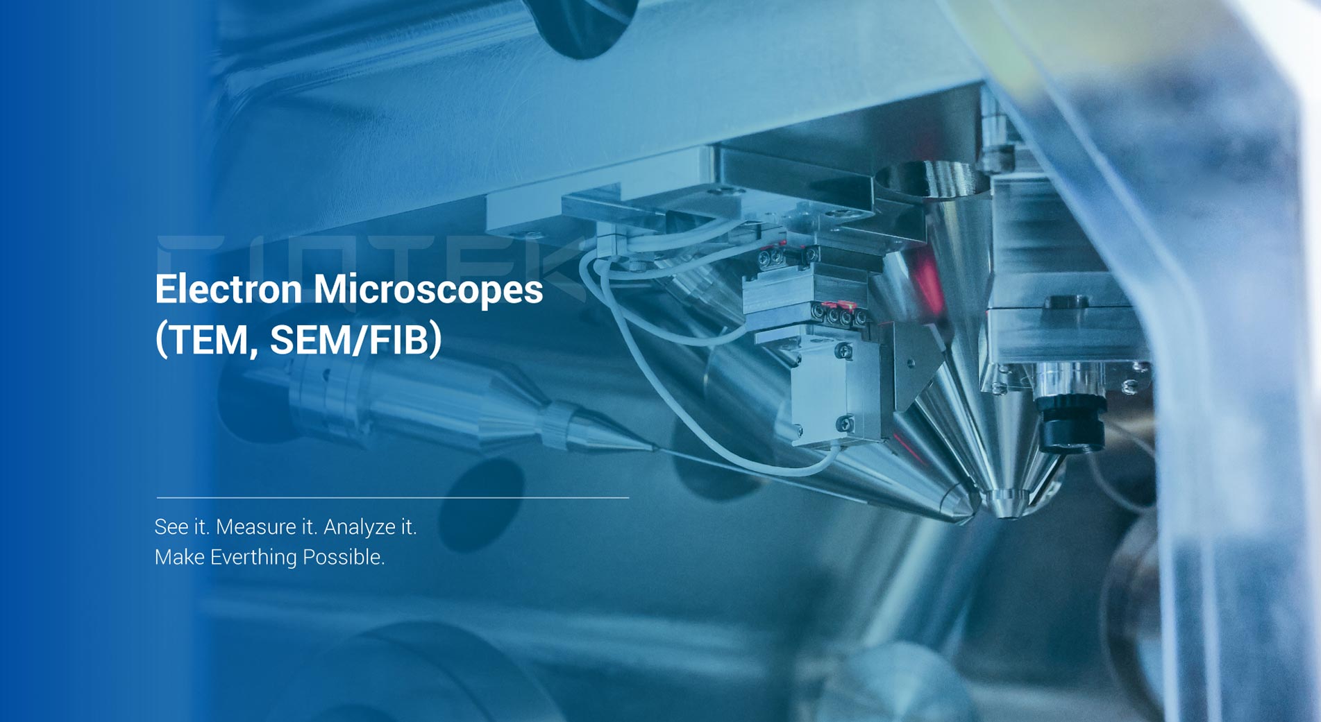
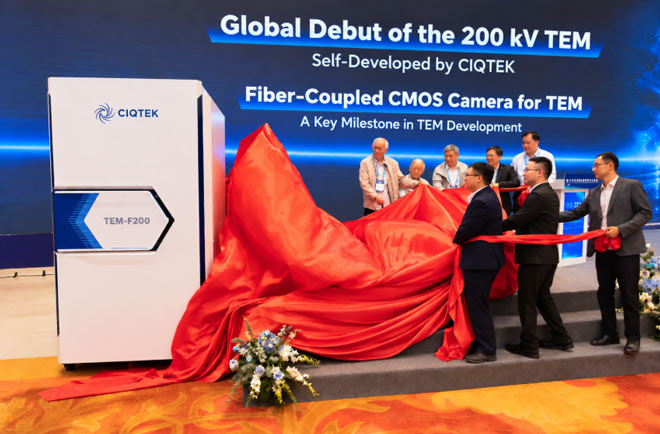
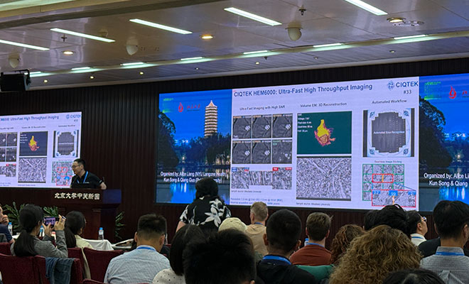
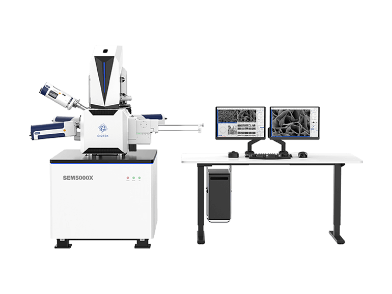
CIQTEK officially unveiled its self-developed TEM-F200 200 kV Field Emission Transmission Electron Microscope at the 2026 National Annual Conference on Electron Microscopy in Nanjing, China. The TEM-F200 was the headline launch among five new electron microscopy products introduced during the event. The new lineup also includes the TEM-F120 120 kV Field Emission TEM, SEM5000Ultra Ultra-High-Resolution Field Emission SEM, a purpose-built fiber-coupled CMOS camera for TEM, and CIQTEK SEM Agent. Together, the launches expand CIQTEK's electron microscopy portfolio from complete microscope systems to imaging hardware and intelligent software. A New 200 kV TEM Developed In-House On October 18, CIQTEK Vice President Dr. Cao Feng introduced the TEM-F200 during a conference presentation focused on the development of CIQTEK's 200 kV transmission electron microscopy technology. The system reaches an information resolution of 0.10 nm. Key components, including the high-voltage power supply, electron gun, constant-power water-cooled objective lens, fully automated apertures, and fiber-coupled CMOS camera, were developed in-house. The TEM-F200 is now ready for volume production and delivery. The launch marks an important step in CIQTEK's expansion into higher-end transmission electron microscopy and strengthens its ability to develop complete electron microscopy systems around core technologies. Five New Products Across TEM, SEM, Imaging and AI Alongside the TEM-F200, CIQTEK introduced four additional products covering different parts of the electron microscopy workflow: TEM-F120, a 120 kV Field Emission Transmission Electron Microscope SEM5000Ultra, an Ultra-High-Resolution Field Emission Scanning Electron Microscope A purpose-built fiber-coupled CMOS camera for TEM CIQTEK SEM Agent, an intelligent software platform for electron microscopy These launches extend beyond individual instruments. They cover complete TEM and SEM systems, core imaging components, and AI-powered software, showing a broader approach to electron microscopy development. From New Instruments to Smarter Microscopy Workflows During the 2026 National Annual Conference on Electron Microscopy, CIQTEK also hosted a series of product sessions covering its TEM portfolio, the new SEM5000Ultra and wider SEM lineup, as well as its AI electron microscopy roadmap and SEM Agent platform. The focus was not simply on adding more instruments. As microscopy workflows become more complex, users increasingly need a combination of high-resolution imaging, stable hardware, automation, and easier operation. By developing complete microscopes, core components, and intelligent software together, CIQTEK is building a more connected electron microscopy platform for materials science, semiconductor research, life science, and other advanced applications. Expanding CIQTEK's Electron Microscopy Platform CIQTEK also worked with seven industry partners during the conference to showcase technologies and ap...
October 20, 2026





 No. 1969, Kongquetai Road, High-tech Zone, Hefei, Anhui, China
 +8615156059133
 info@ciqtek.com














 参加しませんか
 お問い合わせ
 リンクトインページ